
LX discusses Electrostatic Discharge
When working on electronics designs in your workshop, bench or in less than ideal commercial situations there is always the danger of encountering electrostatic discharge (ESD for short). ESD [1] is the sudden flow of electricity between two objects caused by one of three things:
- physical contact – such as simply touching an object with your hand
- an electrical short – due to component or object fatigue
- dielectric breakdown – such as the failure of insulation
Over time it has become easier for those in the semi-professional or hobbyist to not concern themselves as devices and components have become more resistant to the effects of ESD. However this laissez-faire attitude will sooner or later punish the individual’s components or projects. Furthermore, the hazard of ESD is not limited to those with less experience or training, it can affect even the most seasoned engineer.The causes of ESD generally fall into two categories. The first is the familiar static electricity, caused by two objects coming into contact with each other and then separated. A simple example is wearing a sweater made from synthetic materials – you can feel the static electricity as you take the sweater off. The static electricity is caused by a process known as thetribolectric effect, where a charge moves from a highly-charged object to the lower-charged object in order to balance out.The second cause of ESD is electrostatic induction. This is the redistribution of charge in an object, caused by the influence of nearby charges. [2] So you may have an object with an excessive amount of positive charge and bring it close to an object without a charge that can conduct electricity, the electrons in the charged object will be attracted to the other and thus the charge is induced across the gap between the two items.There are several types of ESD, and the most common form is the spark. A spark will occur when the potential difference between two objects is to high the charge will bridge the gap between them. An obvious example of this is lightning – as the potential difference between the charged cloud and the ground is very large. However not all sparks will resemble lightning, and some are small enough to exist yet remain unseen – a hazard in themselves. Some may consider them to be harmless if they’re not strong enough to be visible, however this is not the case.

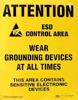
Various risks involved with ESD are documented widely, with the major concern in the electronics design field being the possible damage to electronic components and devices. The most susceptible component types are CMOS integrated circuits and MOSFET transistors. It only tales one careless person to run their hands through their hair and then pick up an IC – only to find it doesn’t work. Why? The high voltage yet tiny static charge transferred from the hair to the hand sparks across to the leg of the IC handled by the engineer, thus rendering it useless. Those parts that are vulnerable to ESD ship in protective tubes, anti-static bags or other special packaging types for a reason, and care needs to be taken once removed from the packaging.So how can these risks be mitigated? The first method involves setting aside an area or converting the work space into an Electrostatic Protective Area (or EPA). To do this the workers need to be grounded, usually via wrist straps; and that all conductive materials are also grounded such as bench mats and surfaces. This can be done easily with the use of anti-static bench and floor mats. Furthermore humidity control is important – by dehumidifying the area involved, the opportunity for moisture to develop on various surfaces decreases and in turn the opportunity for ESD damage. Some organisations may even use ion generators to help neutralise charged surface regions in the space. If you organisation has on-site storage or assembly areas, these will also require various ESD-neutralising systems. Finally the use of appropriate warning signage, staff training and quality control is required to maintain the awareness of ESD and the possible risks.
Even though this has been a summary look at ESD, preparing your organisation can be an expense that isn’t justified when preparing your first design prototype, notwithstanding the cost of setting up a complete electronics design facility and workshop. So if you are thinking about moving into hardware work for the first time, instead consider outsourcing the hardware (or more) prototyping to a team of experts with experience in the field, documented successes and all the resources to successfully move your prototype forward to a product. Here at the LX Group we can partner with you through all stages of the design process, allowing you to avoid the expense of setting up engineering areas in your facility.To get started, simply contact us for a confidential discussion about your ideas and how we can help bring them to life – click here to contact us, or telephone 1800 810 124.LX is an award-winning electronics design company based in Sydney, Australia. LX services include full turnkey design, electronics, hardware, software and firmware design. LX specialises in embedded systems and wireless technologies design. https://lx-group.com.auPublished by LX Pty Ltd for itself and the LX Group of companies, including LX Design House, LX Solutions and LX Consulting, LX Innovations.[1] ESD definition Wikipedia, accessed 09/11/2012 http://en.wikipedia.org/wiki/Electrostatic_discharge
[2] Electrostatic induction definition from Wikipedia, accessed 09/11/2012 http://en.wikipedia.org/wiki/Electrostatic_induction
From making ideas real, to scaling their capability.
Have a project you’d like to discuss? Speak to our team today.
.avif)