All posts tagged: embedded

The fact that the Internet of Things shows a lot of promise both now and in the future is certain – and your customers, designers and the public will have an almost limitless amount of ideas with regards to new products and their implementation. However when the time comes to select the hardware to drive these innovations, choosing from one of the wireless chipsets can be a minefield – and more so when WiFi is involved.

802.11 wireless LAN is an attractive technology for building networks of wireless sensors and embedded devices due to its widespread use and the availability of nearly ubiquitous existing network infrastructure. Let’s take a look at a few existing chipsets on the market today that can be used to add wireless networking to existing embedded designs with relatively low complexity and cost.

First there’s the RN131 802.11b/g WiFi module by Roving Networks – a complete low-power embedded networking solution. It incorporates a 2.4 GHz radio, processor, TCP/IP stack, real-time clock, crypto accelerator, power management and analogue sensor interfaces into a single, relatively power-efficient module. In the most simple configuration, the hardware requires only 3.3V power, ground, and a pair of serial UART lines for connection to an existing microcontroller, allowing wireless networking to easily be added to an existing embedded system.

The module incorporates a U.FL connector for connection of an external antenna, without any microwave layout or design needed to use the module. This module has a current consumption of 40mA when awake and receiving, 200mA when actively transmitting, and 4µA when asleep, and the device can wake up, connect to a WiFi network, send data, and return to sleep mode in less than 100 milliseconds. This makes it possible to achieve a runtime on the order of years from a pair of standard AA batteries – an ideal solution for power-efficient, battery powered wireless sensor network and Internet-of-Things solutions.

fbd_swrs126

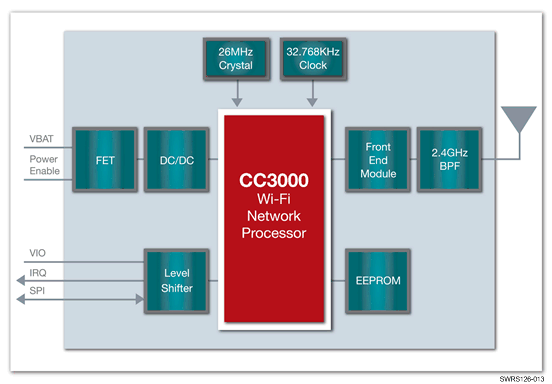
Next there’s the Texas Instruments CC3000 Wireless Network Processor – which allows WiFi to be added to any existing microcontroller system relatively easily, and at a low cost. The CC3000 integrates an entire IPv4 TCP/IP stack, WiFi driver and security supplicant on the chip, making it easily portable to lightweight microcontrollers without the memory burden of implementing a TCP/IP stack in the host microcontroller where relatively low-power, low-cost microcontrollers such as 8-bit AVR or PIC devices are used. And this compact module measures only 16.3mm x 13.5mm.

CC3000 reference designs available from TI demonstrate chip-antenna based designs that are already FCC, IC and CE certified, which can make it easier to develop bespoke solutions that can pass compliance testing for products going into markets where such compliance is needed. The CC3000 requires no external crystal or antenna balun, and in fact requires almost no external components at all except for an SPI interface to the host microcontroller and an antenna – and the device costs less than $10.

The flexible 2.7-4.8V power supply requirement offers great flexibility when combined with battery power or energy harvesting solutions. However, this chip is not a PCB-based module, meaning that a 50 ohm 2.4 GHz antenna must be added externally – so the designer must have a little familiarity with microwave design, such as microstrip transmission line layout and the choice of the right antenna connector. However, this offers the designer complete flexibility to choose the most appropriate antenna type for the size, range and gain requirements of the design – a larger external antenna, a compact chip antenna, or a microstrip antenna fabricated on the PCB with no bill-of-materials cost.

Our final subject is the Redpine Signals’ Connect-IO-n series of modules which allow 802.11 wireless LAN connectivity to be added relatively easily to an embedded microcontroller system. In collaboration with Atmel these modules have been optimised for use with Atmel microcontrollers, particularly the Atmel AVR XMEGA and AVR UC3 series microcontrollers.

Some modules in this family provide 802.11a/b/g/n Wi-Fi connectivity, whilst all modules provide the TCP/IP stack on board and are FCC certified, making RF compliance certification of your entire design easier. These modules are aimed at providing the ability to add 802.11 wireless connectivity to 8-bit and 16-bit microcontrollers with low integration effort and low memory footprint required in the host microcontroller to support the WiFi device, especially where 802.11n support is desired.

Like the other chipsets we’ve discussed, the modules in this series can be interfaced to the host microcontroller over a UART or SPI interface, and similarly to their competitors, a standby current consumption of only a few microamps potentially allows for years of battery life with no external energy source as long as the radio is only briefly enabled when it is needed.

The RedPine RS9110-N-11-28 module from the Connect-IO-n family in particular is relatively unusual in that it provides dual-band 2.4GHz/5GHz 802.11 a/b/g/n connectivity for your embedded device – supporting connection to any WiFi device or network and potentially avoiding congestion in the 2.4 GHz band as used with 802.11b/g devices.

2

Whilst 802.11n offers a significant increase in the maximum net data rate from the 54 MBit/s of 802.11b/g to 600 Mbit/s, do you really need 600 Mbit/s of data to your wireless sensor network or embedded appliance? I doubt it. However, one case where you might want an 802.11n radio supporting operation in the 5 GHz spectrum for your wireless sensor network device is if your wireless LAN infrastructure is a pure 5 GHz 802.11n network – whilst this breaks compatibility with legacy devices, it delivers maximum network performance.

As you can see the possibilities for low-power connected devices are plentiful and the hardware is available on the open market. It’s then up to your team to turn great ideas into great products. Furthermore modifying existing products to become connected is also a possibility. However if wireless or Internet-connectivity is new to your team – and you’re in a hurry, have a reduced R&D budget, need guidance or want to outsource the entire project – it can be done with the right technology partner.

Here at the LX Group we have the experience and team to make things happen. With our experience with connected devices, embedded and wireless hardware/software design, and ability to transfer ideas from the whiteboard to the white box – we can partner with you for your success.

We can create or tailor just about anything from a wireless temperature sensor to a complete Internet-enabled system for you – within your required time-frame and your budget. For more information or a confidential discussion about your ideas and how we can help bring them to life – click here to contact us, or telephone 1800 810 124.

LX is an award-winning electronics design company based in Sydney, Australia. LX services include full turnkey design, electronics, hardware, software and firmware design. LX specialises in embedded systems and wireless technologies design. https://lx-group.com.au

Published by LX Pty Ltd for itself and the LX Group of companies, including LX Design House, LX Solutions and LX Consulting, LX Innovations.

Muhammad AwaisLX Group examines wireless chipsets for IoT devices

Wearable computing – the use of personal computers, displays and sensors worn on one’s person – gives us the potential for advancement in human-computer interaction compared to traditional personal computing – for example the ability to have constant access and interaction with a computer – and the Internet, whilst going about our daily activities.

This could be considered the ultimate in multitasking – the use of your computing device at any time without interrupting your other activities. For example, the ability to read an email or retrieve required information while walking or working on other tasks. Wearable computing potentially offers much greater consistency in human-computer interaction – constant access to the computer, constant connectivity, without a computing device being used in an on-and-off fashion in between other activities.

glass1

Once contemporary example of this is the new Google Glass, which represents an advanced, sleek, beautifully designed head-mounted wearable computer with a display suitable for augmented-reality applications – or just as an “ordinary” personal head-mounted display. Even before its public release, the frenzy surrounding Google Glass amongst technology enthusiasts demonstrates the potential level of market demand for wearable computers.

However, with a price of at least US$1500 price tag of Google Glass, (at least for its “Explorer Edition” beta version) this leads many to consider what potential might exist for the deployment of wearable computing and wearable sensor-network technologies – however at a lower cost.

One example is the category known as “Smart Watches” such as the Sony SmartWatch and Pebble Technology’s “Pebble” e-Paper watch – which both offer constant, on-the-go access to information from the Internet – and thus become a member of the Internet of Things – at a glance of the wrist. Text messages and email notifications are amongst the most simple, common examples of data that can be pushed to a smart watch, but the display of information from a multitude of other Internet-connected data streams is possible.

With the growing popularity and increasing hardware capabilities of smart phones, it is increasingly taken for granted that a smart phone carried on one’s person can act as a gateway between the Internet (connected via the cellular networks) and other smaller, lower-power wearable computer or sensor devices worn on the body and connected back to the smartphone via standard data links such as WiFi or Bluetooth. In using the smart phone as an Internet connection, the size, price and weight of the wearable device can be significantly reduced – which also leads to a considerable reduction in cost.

Furthermore, apart from providing mobile Internet connectivity, the smart phone can also provide a large display and an amount of storage capacity – which can be harnessed for the logging, visualisation and display of data collected from a network-connected sensor node wearable on one’s body, or a whole network of such sensor nodes distributed around different personal electronic devices carried on the person and different types of physical sensors around the body.

The increasing penetration of smart phones in the market and the increasing availability and decreasing cost of wireless radio-networked microcontroller system-on-chips, MEMS glass2
sensors and energy efficient short-range wireless connectivity technologies such as Bluetooth 4.0 are among some of the factors responsible for increasing the capabilities of,
and decreasing the cost of, wearable computing and wearable Internet-of-Things and sensor platforms.

Speed and position loggers, GPS data loggers and smart pedometers intended for logging and monitoring athletic performance, such as the Internet-connected, GPS-enabled,
Nike+ system; along with biomedical instrumentation and sensor devices such as Polar’s Bluetooth-connected heart rate sensors are other prominent examples of wearable Internet-of-Things devices which are attracting increasing consumer interest on the market today.

Combined with display devices such as smart watches, smart phones and head-mounted displays such as Google Glass. these kinds of wearable sensors create a complete wearable machine-to-machine Internet-of-Things network that can be self-contained on one’s person. Which leads us to the next level of possibilities – what do your customers want a device to do? And how can it be accomplished? And do you have the resources or expertise to design, test and bring such a system to the market?

It isn’t easy – there’s a lot of technology to work with – however it can be done with the right technology parter. Here at the LX Group we have the experience and team to make things happen. With our experience with sensors, embedded and wireless hardware/software design, and ability to transfer ideas from the whiteboard to the white box – we can partner with you for your success.

We can create or tailor just about anything from a wireless temperature sensor to a complete Internet-enabled system for you – within your required time-frame and your budget. For more information or a confidential discussion about your ideas and how we can help bring them to life – click here to contact us, or telephone 1800 810 124.

LX is an award-winning electronics design company based in Sydney, Australia. LX services include full turnkey design, electronics, hardware, software and firmware design. LX specialises in embedded systems and wireless technologies design. https://lx-group.com.au

Published by LX Pty Ltd for itself and the LX Group of companies, including LX Design House, LX Solutions and LX Consulting, LX Innovations.

Muhammad AwaisWearable Computing and the IoT

Recently an increasing number of networked devices are finding their way into consumer, industrial and medical applications. Such networks often employ distributed nodes which cannot practically be connected to the power grid – through design or through necessity. Therefore powering such devices can possibly be a challenge – due to the costs of either running from battery or solar power, sending technicians for maintenance visits to replace batteries – or having to install one’s own power network for the IoT system.

This is where energy efficiency is key – by using highly energy-efficient design practices in both the hardware and software levels, the power requirements can usually be reduced significantly. In doing so the power supply paradigm can be altered to one of lower cost and higher efficiency. Especially for remote or portable devices that use RF/microcontroller chipsets – the smaller the power requirement the better.

ee2

High-power and efficient wireless network nodes can be engineered using modern RF microcontroller system-on-chip devices, activating sensors and peripheral hardware devices only when they are required, and then putting them into low-power sleep modes when not in use. Similarly, the RF transceiver can be switched into a very-low-power sleep state until the microcontroller decides that a transmission of collected sensor data is required. The microcontroller can then wake up the radio, perform the required transmission, and then revert to sleep mode.

In some cases, a burst of data transmission across the wireless network might only occur when a small, intermittent energy-harvesting power supply has accumulated enough energy in a capacitor to power a transmission. Alternatively, a low-power wireless sensor node can “wake-on-radio”, only taking the microcontroller out of its sleep state when a message is received over the wireless network requesting a sensor readout and only powering up the sensors and microcontroller at this time.

With most of the components of the system, such as the microcontroller, radio and sensors – each kept off-line or asleep for the largest practical amount of time – efficiently designed wireless sensor nodes may achieve operating timescales as long as years off a single battery. Today’s typical wireless RF microcontroller system-on-chips targeted at IoT applications typically consume about 1-5 microwatts in their “sleep” state, increasing to about 0.5-1.0 mW when the microcontroller is active, and up to around 50 mW peak for brief periods of active RF transmission.

However when considering the design of energy-efficient, low-power IoT sensor networks, it can sometimes be advantageous to think not just in terms of power consumption, but in terms of the amount of energy required to perform a particular operation. For example, let’s suppose that waking up a MEMS accelerometer from sleep, performing an acceleration measurement and then going back to sleep consumes, say, 50 micro joules of energy; or that waking up an RF transceiver from sleep, transmitting a burst of 100 bytes of data and then going back to sleep consumes 500 micro joules.

If we know the specific energy consumption of each operation, then the average power consumption is simply the energy per operation multiplied by the frequency of that operation, summed over the different kinds of operations. Of course, this assumes that the continuous power consumption of each device when it is asleep is very small and can be ignored. Alternatively, if we have a certain known power budget available and a known energy budget for each sensing, computation or transmission operation – we then know the maximum practical frequency at which a sensor node can perform sensor measurements and transmit its data.

ee

Additionally, efficient wireless sensor nodes can take advantage of some form of energy harvesting power supply – employing energy sources such as solar cells, vibrational energy harvesters or thermoelectric generators to minimise maintenance and extend battery life – with the possibility of completely eliminating external power supplies, but only if the power consumption of the system is small enough and a capacitor is employed for energy storage.

In many applications, solar cells are the most familiar and relatively mature choice for low-power network nodes operating outdoors or under good indoor light conditions. However, other technologies suitable for extracting small amounts of power from the ambient environment exist. For example, a wireless sensor node set up to monitor bearing wear in a generator could employ a piezoelectric crystal as a vibrational energy harvester, converting motor vibration into usable energy, or a thermoelectric generator mounted on a hot exhaust could harvest a small amount of otherwise wasted energy from the thermal gradient.

Typical vibrational energy harvesters usually operate with a cantilever of piezoelectric material that is clamped at one end and tuned to resonate at the frequency of the vibration source for optimal efficiency – although an electromagnetic transducer can be used in some cases. Whilst the electrical power available is dependent on the frequency and intensity of the vibrations, the cantilever tip mass and resonant frequency can generally be adjusted to match the machinery or system that energy is to be harvested from.

Furthermore, energy harvesting management ICs that manage the accumulation of energy in a capacitor over a period of time can enable short bursts of relatively high power consumption, such as when a node wakes up and transmits a burst of data, and are particularly well suited to low-power wireless sensor nodes.

Even with the examples mentioned above, the energy-efficiency possibilities are significant and can be a reality. When designing prototypes or proof-of-concept demonstrations you may put energy use to one side, however when it comes time to generate a real, final product – you can only benefit from taking energy-efficiency into account.

If you are considering creating or modifying existing designs and not sure about the energy-saving and generating options that are available, be efficient and discuss your needs with an organisation that has the knowledge, experience and resources to make your design requirements a reality such as here at the LX Group.

At the LX Group we have a wealth of experience and expertise in the embedded hardware field, and can work with the new and existing standards both in hardware and software to solve your problems. Our goal is to find and implement the best system for our customers, and this is where the LX Group can partner with you for your success.

We can create or tailor just about anything from a wireless temperature sensor to a complete Internet-enabled system for you – within your required time-frame and your budget. For more information or a confidential discussion about your ideas and how we can help bring them to life – click here to contact us, or telephone 1800 810 124.

LX is an award-winning electronics design company based in Sydney, Australia. LX services include full turnkey design, electronics, hardware, software and firmware design. LX specialises in embedded systems and wireless technologies design. https://lx-group.com.au

Published by LX Pty Ltd for itself and the LX Group of companies, including LX Design House, LX Solutions and LX Consulting, LX Innovations.

Muhammad AwaisEnergy efficiency for the Internet-of-things

As mentioned in our previous discussion of the 4-20 mA current loop, there are many forms of wired data transmission that can be used in products, and today we’d like to review another form – the Inter-integrated Circuit bus (or I2C bus for short). This is also known as the “two wire interface” and has been around for quite some time. Invented by NXP (previously Philips Semiconductor) the I2C bus is a multi-master serial single-ended data bus used to allow systems to communicate with a huge variety of electronic devices.

From a hardware perspective it is quite simple – each device connects to the serial data and clock lines, which are controlled by the master device. The clock and data lines are connected to Vdd via pull-up resistors, for example:

 The master device controls the bus clock and initiates communications with each slave device. Communications are initiated by sending the slave device address – which is unique to each device – and then either data write or request commands. Then the slave device will act upon received data, or broadcase the required number of bytes of data back to the master device.

You may be wondering how the slave addresses are organised – each device manufacturer applies for an address range from NXP for their products. Some devices will only have one set address, and some can have their address altered – for example by changing the last three bits in the binary representation of the addresses. This is done in hardware by connecting three pins to Vdd or GND.

The speed of the I2C bus varies, and can range from 10 kbps to 3.4Mbps – with the speed usually proportional to the total device power requirements. The usual speed for the majority of devices is 100 kbps.

The decision to use the I2C bus can be simple, due to the popularity of the interface even on the most inexpensive of microcontrollers – and many design engineeers are familiar with the bus due to the history.

But what sort of devices can make use of the I2C bus? There are literally thousands available, in a wide range of categories. These can include simple temperature sensors, EEPROMS, motor controllers, LCD interfaces, I/O expanders, real-time clocks, UART interfaces, ADC/DACs, and more.

Apart from the huge range of devices, the advantages of using the I2C bus include industry expertise, the ability to address literally hundreds of devices using only two master I/O pins, and that devices on the bus can be “hot swap” – that is you can add or remove devices from the bus without powering off the entire system. This in itself is perfect for systems with maximum run-time requirements, as technicians can replace faulty device modules with reduced down-time for the end user.

However there are disadvantages to the I2C bus, two of which need to be taken into consideration. The first is that the maximum physical length of a bus run is usually around 20 metres, and in some cases much less. You can use bus extension devices from NXP (and others) that will allow much further physical distances – however designers need to ensure the capacitance across the bus stays at around 400 picofarads.

The second disadvantage is the possibility of slave address clash. You may have two specialised devices with the same slave address. In these situations you need to use an address multiplexer IC on the bus which first needs to be controlled, and then the device selected is addressed as normal. Nevertheless, as part of normal prototyping and planning these disadvantages can be removed or minimised with appropriate engineering.

It can be said that the I2C data bus may not be the “latest technology”, but it can effectively solve problems in the right circumstances. However there are many options, and choosing the right one is a fundamental step for the success of your project. So if your design team is set in their ways, or you’re not sure which data communication method is best for your application – it’s time to discuss this with independent, experienced engineers.

 At the LX Group we have experience designing a wide range of data gathering and control systems over short and long distances – and using this experience we can determine the most effective method of returning data and control signals no matter the application or geography. Our engineering team have developed a number of systems in this area and have extensive experience with the core technology requirements of such systems.

We understand the importance of high availability, accuracy and integrity of the systems, combined with the need for future proofing infrastructure rollouts. For more information or a confidential discussion about your ideas and how we can help bring them to life – click here to contact us, or telephone 1800 810 124.

LX is an award-winning electronics design company based in Sydney, Australia. LX services include full turnkey design, electronics, hardware, software and firmware design. LX specialises in embedded systems and wireless technologies design. https://lx-group.com.au  Published by LX Pty Ltd for itself and the LX Group of companies, including LX Design House, LX Solutions and LX Consulting, LX Innovations.
Muhammad AwaisLX Group discusses the Inter-integrated Circuit Bus

Building prototypes of your product idea during the design process is naturally important and something that is a necessity for many reasons – including physical conceptualisation, demonstrations to possible financiers, proof of concept, usability testing in later stages, and project inspiration. However like all stages of the design process (as discussed last week) doing so requires a level of knowledge and expertise that not every organisation possess.

 This is not a criticism, but should be taken as a positive observation. And like any skill – if you can’t do it properly yourself, find someone who can. Here at the LX Group we will take the time to understand your needs and ideas which can then be transformed into one or even a range of prototypes – setting you up for success. As part of this process a decision needs to be made with regards to the type of prototype required, so let’s examine them in more detail and the benefits of each.

 Proof-of-concept prototypes

This is often a very basic example that will function in a similar manner to the final product – to prove that it is feasible and can be done. We say that the key purpose is to focus on, understand and address identified risk areas with the prototype. For example selecting an appropriate microcontroller to ensure processing speed and I/O requirements are adequate, or power consumption levels fall under a required maximum. During this level of prototyping it is important to remove design faults and technical risks otherwise the costs involved to make changes later on will be exponential compared to doing so now.

 Demonstration prototypes

When you need to show someone what “it’s all about” – a demonstration prototype will be required. This is the model you shop around to potential investors and future customers, document or show during grant applications, and generally spruik to the outside world. Those of you in larger organisations may also require this to “sell” the concept to decision makers in the upper echelons of management. The prototype may not function as the final product, however it should appear to do so. For example the housing and cosmetic look will match the final product as much as possible, however embedded software may be very basic or “emulate” the required functions.

 Research and Development prototype platforms

When you have the go-ahead to move forward with the project design, it’s time to get working on the design – which requires R&D prototypes. The algorithm development of the product can take place with these prototypes, and thus may not look like the finished product, but they will have the functionality and specified hardware to operate as one. Furthermore this type of prototype may be modified or altered during the research process to account for changes, updates and possible design changes.

 Commercial Product Iterations

There are three iterations during this stage in the design process, including:

  • Alpha prototypes – these are the first revision of the design and generally meet all aspects of the product design. These will be used to test the design parameters, review the design and seek improvements, and seek internal suggestions and improvement ideas.

  • Beta prototypes – these will include any changes made during the alpha prototype stage, and be submitted for compliance testing, certification, stress testing and product trials. After the results of those operations more changes may be required to the design requirements and specifications.

  • Pre-production prototypes – these are manufactured during short runs and ideal for verifying the manufacturing process, component suppliers, determining production yields, product testing, and the supply chain. For more popular products security at all stages of the supply and manufacturing chain is vital to remove the possibility of information leaks, industrial espionage and intellectual-property theft. You don’t want fuzzy photos of your next great thing plastered over Internet pundit websites.

 Where to from here?

 Your project budget and prototype requirements will determine the method of creation and time required to do so. For many designs the speed of prototyping can be increased dramatically, in conjunction with reducing the budget requirement by using a mixture of standard components, development kits, a mixture of reference and custom designs and pre-designed hardware libraries. By not “reinventing the wheel” wherever necessary time and money can be saved without too much effort, leaving resources available for R&D or custom sections of the design.

 So if you have an idea for a prototype and not sure about how to move forward and would like to have an experienced organisation take care of everything – we can “make it happen”. At the LX Group we have our own hardware compiler – a proven system of product design that will save you precious time and money. No matter what stage of design your team has achieved, we can partner with you to share our design and manufacturing expertise for your benefit.

 To move forward with your prototype requirements, simply contact us for a confidential discussion about your ideas and how we can help bring them to life – click here to contact us, or telephone 1800 810 124.

 LX is an award-winning electronics design company based in Sydney, Australia. LX services include full turnkey design, electronics, hardware, software and firmware design. LX specialises in embedded systems and wireless technologies design. https://lx-group.com.au

 Published by LX Pty Ltd for itself and the LX Group of companies, including LX Design House, LX Solutions and LX Consulting, LX Innovations.

Muhammad AwaisLX Group – your Partner for Prototyping

When fighting a warehouse fire in extraordinary temperatures, you don’t want to worry about the two-way radio breaking down. If a police car is broadsided during a high-speed chase, the on-board computer can’t be torn free to become a dangerous projectile. When staking out a remote location in the desert or on or drilling for oil in the North Sea, electronic equipment needs to withstand the extreme weather.

When designing projects for extreme environments such as the previous examples, you need rugged electronic designs. To make sure your clients and end users in the field have technology they can rely on, a number of organisations have developed stringent industry testing standards and procedures. This has an impact on product design as engineers are required to know, design and test their equipment to comply with set standards. The desired end here is for the products to survive “Torture Tests” and gain compliance certificates.

Ruggedisation is defined as “designed or improved to be hard-wearing or shock-resistant. There are four categories of rugged electronic equipment; commercial-grade; durable; semi-rugged and fully rugged. Today’s most widely used ruggedness standards include those from four highly respected sources: the International Electrotechnical Commission (IEC), the European Committee for Electrotechnical Standardisation (CENELEC) which publishes the European IP (Ingress Protection) standards for electrical equipment, and the United States military.

Most standards provide exceptionally detailed instructions and procedures for product testing. Major tests normally performed include:

  • Water Intrusion: When water or rain penetrates a device, they can cause short circuits and corrosion. Many manufacturers test their rugged products against both MIL-STD-810F and IP54, IP64, IP66 water and rain intrusion standards. Testing for rain intrusion is normally done in a rain chamber that drenches products with jets of water of varying intensities from all possible angles, as well as for dripping water for different periods of time. Fully rugged models are also tested with full immersion, to IP68 and MIL-STD-810F, Method 512.4.
  • Salt and Fog: In coastal and marine environments, salt and fog can cause electronic equipment to short circuit or rust, affecting performance both short and long-term. Engineers normally test to the MIL-STD-810F Method 509.3 standard using the specified five percent saline solutions.
  • Humidity: Conditions of extreme humidity can cause electronic devices to corrode and malfunction over time. Typical tests are to MIL-STD-810F Method 507.3 specifications, which specify 95 percent relative humidity and worst-case scenario high temperatures up to 75°C.
  • Dust Intrusion: Dust and sand intrusion in deserts, shorelines, mines, construction sites, or other environments can cause movable parts like buttons and keypads to clog and malfunction. Often manufacturers test to both MIL-STD-810F, Method 510.3 for sand and dust testing and IP standards for blowing dust.
  • Drop Testing: In the field, it’s common for handheld devices to be knocked over or dropped. Manufacturers test to MIL-STD-810F Method 516.5 with around 90- to 120 cm free-fall drops to concrete, and also with tip-over tests. The equipment is expected to remain fully operational after multiple drops.
  • High and Low Temperatures: Manufacturers test their technology under operating conditions of minus 35°C (MIL-STD-810F Method 502.3) and plus 60°C (MIL-STD-810F 501.3). In addition, equipment is often stored under extreme temperature conditions, and is expected to work to specification when put into service. Many manufacturers tests equipment storage in extreme low temperatures down to minus 57°C (also MIL-STD-810F Method 502.3) and high temperatures up to 85°C (also MIL-STD-810F 501.3).
  • Temperature Shock: Equipment is often transported by aeroplane, or used outdoors and brought inside, meaning it can be under extreme cold for long periods of time, then deposited or stored in extreme heat. Equipment is tested under these precipitous temperature fluctuations to MILSTD- 810F Method 503, testing equipment that has gone from storage of minus 57°C to 80°C and vice versa.
  • Sun Exposure: Equipment that is installed in, or must work in, unrelenting sunshine is tested to MIL-STD-810F Method 505.4 standards for enclosure and performance damage from solar radiation. Tests normally last from three to seven days, and are conducted in a specially designed solar chamber.
  • Shock and Crash Testing: Mobile and vehicle mounted products are tested to make sure they are installed correctly by subjecting them to worst-case scenario accident impact tests. MILSTD- 810F Method 516.4 tests are exceptionally stringent. Equipment must continue to operate correctly under 75Gs, or 75 times the force of gravity. Drop tests of varying heights to a steel floor are also conducted. Equipment must stay intact, mounted and continue to be 100 percent functional.
  • Vibration: Vibration testing to MIL-STD-810F Method 514.5 measures how equipment reacts to different levels of vibration, which can cause wire chafing, intermittent electrical contacts, display misalignment and other issues. Tests are conducted in both standard vehicles such as cars and trucks and under the more severe vibrations caused by more vibration-prone vehicles such as motorcycles, tanks and others.
  • Low Pressure: High altitudes and dropping pressure, such as in aircraft or on mountains, can cause membranes in parts such as speakers, microphones and keypads, to malfunction. Manufacturers conduct low-pressure performance tests to MIL-STD-810F Method 500.3 that ensure 100 percent equipment functionality

To ensure that products go to market quickly and don’t suffer costly delays, engineers should include relevant testing consideration as part of the design process. By confirming assumptions of the product’s compliance—such as the market and classification of the area in which the equipment will be used (Class I, Division 1, Class I, Zone 0 etc.), determining the appropriate protection concept (intrinsic safety, flame-proof, etc.), and establishing the indicative environmental considerations (enclosure ratings, extended ambient temperature range and so on) product development will be smoother and not require reworking to meet aforementioned standards.

The recommendation is for engineers proceeding into research and development stages to keep the submission for final certification in mind. This could mean reaching out to consultants who will help you through your submission process and follow their advice and guidelines.

At the LX Group we can carry out product testing, verification and compliance certification. We also partner with a number of NATA-certified local and international partners to provide independent product compliance and environmental testing.

LX has a range of equipment to support environmental and certification testing including an environmental test chamber, EMC test equipment, ESD simulator (CE testing), and various electrical input simulation devices such as environmental testing, design verification and compliance testing.

Some common compliance standards include:

  • EMC emissions and immunity testing (including C- Tick, FCC and CE)
  • Electrical safety (mains certification)
  • UL certification
  • RoHS and WEEE compliance
  • Industry-specific standards (including medical and mining)
  • Ingress Protection (IP) rating
  • Packaging and labelling requirements

For more information or a confidential discussion about your ideas and how we can help bring them to life – click here contact us, or telephone 1800 810 124.

LX is an award-winning electronics design company based in Sydney, Australia. LX services include full turnkey design, electronics, hardware, software and firmware design. LX specialises in embedded systems and wireless technologies design. www.lxgroup.com.au

Published by LX Pty Ltd for itself and the LX Group of companies, including LX Design House, LX Solutions and LX Consulting, LX Innovations.

Muhammad AwaisDesigning embedded hardware to withstand rugged environments