All posts tagged: Hardware

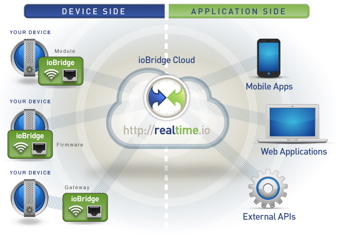
When considering methods of adding Internet-of-things connectivity to existing or new ideas, being able to integrate open-source hardware can help reduce hardware target costs, however support and development advice can be lacking due to the distributed nature of open hardware development.

However with the openPicus ecosystem, we have found an inexpensive hardware choice that is also fully supported by the manufacturer and also allows for integration into final, closed products. The openPicus ecosystem provides user-friendly Internet connectivity for the relatively easy development of Internet-of-Things applications.

openPicus is based around the openPicus Flyport family of low-power, network-connected microcontroller modules, which are available in three different versions, with either Wi-Fi, GPRS or Ethernet connectivity but with the same microcontroller and an otherwise equivalent module pinout.

Each Flyport module is pinout-compatible, allowing the same underlying hardware design to be assembled with different Flyport modules to meet changing connectivity needs that your customer may have. All Flyport modules are based around the same Microchip PIC24FJ256 16-bit PIC microcontroller, making firmware development easily portable across the different modules.

openPicus provides an IDE, comprehensive documentation, tutorials and a consumer discussion forum for its products, aimed at enabling developers of cloud services and mobile apps to use the system to prototype and develop Internet-connected hardware solutions relatively easily with minimal electronic engineering expertise.

Flyport is an open platform, providing an embedded webserver (for the Wi-Fi and Ethernet-connected modules), support for both infrastructure and ad-hoc Wi-Fi network modes (for the Wi-Fi version of the module) and sleep and hibernate modes for efficient power use when operating from batteries.

Each of the Flyport modules provide up to 18 digital I/O pins for interfacing to external hardware, four 10-bit ADC input pins, 4 UARTs, SPI and I2C interfaces. The Ethernet and Wi-Fi versions of the Flyport modules include two megabytes of external flash memory on board, and all versions include an internal real-time clock in the microcontroller.

The Flyport modules are all powered by the openPicus framework, which is itself based on the FreeRTOS real-time operating system. An IDE is provided, free, to make it easy to develop your own applications running on top of Flyport technology. Flyport modules are programmed using a C or C++ like programming language, with Flyport making development easy by managing all the required network interfacing, Internet communications protocols and the webserver internally for you.

The API allows management and programming of all the available functionality of the entire family of Flyport hardware modules, allowing the developer to import web pages, create applications, compile and download code to Flyport modules. Unfortunately, the IDE is only available for Windows at this time, although it can be run inside a virtual machine (with Windows installed) on OSX or Linux PCs.

Most of the underlying technology of the openPicus / Flyport system is released as open source software and open hardware, but with licensing choices such that you are not forced to release all your own code under an open-source license if you choose not to when integrating openPicus technology into your own commercial designs.

The openPicus Flyport IDE has its source code released under the GPLv3 license, and the schematics for the Flyport hardware are released under the CC-BY 3.0 Creative Commons license. Using the openPicus core, libraries and code samples in the firmware of your commercial product does not require you to release the source code of your firmware, provided that the core and libraries are used without modification.

If you tweak or modify the openPicus core or libraries then you are required to release the modified code under the LGPL v3.0 license.openPicus provides their code samples, applications, example projects and libraries for open use under the Apache 2.0 license, and the openPicus Framework (including the TCP/IP stack, email and FTP support) under an LGPL v3.0 license.

openpicus

A number of pre-designed carrier boards for Flyport modules are available, allowing development with easy-to-use hardware “building blocks” with little or no expertise in custom electronic hardware design and construction required.

For example, the Music Nest is a carrier board for Flyport modules which can be used to develop Internet-connected audio applications. A VLSI1053 stereo audio codec IC is onboard, interfaced back to the Flyport module over SPI, along with an SD card for the storage of audio files.

Another example is the “Grove Nest” carrier board is a simple carrier board for Flyport modules that provides 10 ports for sensors and other peripheral modules which are compatible with Seeed Studio’s “Grove” connector standard. openPicus provides example libraries for a large range of sensor and actuator devices from Seeed’s “Grove” family of development modules, allowing the development of Internet-connected, Internet-of-Things devices in an easy “plug and play” fashion with minimal hardware expertise.

As is typical of Arduino and most similar development boards, these Flyport carrier boards can be powered either via an external power supply or via the same USB connector which is used to download firmware to the Flyport module. The Ethernet Flyport module is a programmable system-on-module based around the 16-bit PIC microcontroller common to all Flyport hardware, combined with a fully integrated 10/100 ethernet interface with integrated MAC and physical layer and a unique MAC address pre-configured for each module.

By default the Ethernet Flyport module includes an RJ-45 ethernet jack, but you can also route the Ethernet signals off the module to an RJ-45 jack on the carrier board, providing flexibility in terms of where the bulky RJ-45 connector is located on your board. Using the Flyport Ethernet module provides the embedded system with a powerful “Internet engine” with a small footprint, low power consumption and low cost, allowing real-time control and display of data on a dynamic webpage accessible from a standard web browser, from a PC, tablet or smartphone.

Thanks to the embedded webserver built into Wi-Fi and Ethernet Flyport modules – they can host HTML pages directly, allowing easy access to information such as sensor readings (or a user interface for control of hardware devices) using an internal webpage. Display of dynamic webpage content in the form of Javascript and Ajax is also supported.

Finally the TCP/IP stack and the application layer run on the main microcontroller of the Ethernet and Wi-Fi Flyport modules, meaning that you have full control of the connectivity and the application.

This means you can, for example, process data coming in from sensor hardware and display this data on a webpage served up from the Flyport module, or send the data to a remote location via email or FTP. You can also shut down the Wi-Fi or Ethernet connectivity to reduce power consumption when connectivity is not actively required.

The openPicus system provides a well-documented and easy method of integrating IoT connectivity into existing and new products, and thus helps decrease the time to market for your new and existing products.

With our experience in embedded hardware, IoT-connectivity and complete product design – we can partner with you for every stage of product development to meet your needs. As we say – “LX can take you from the whiteboard to the white box”. So for a confidential discussion about your ideas and how we can help bring them to life – click here to contact us, or telephone 1800 810 124.

LX is an award-winning electronics design company based in Sydney, Australia. LX services include full turnkey design, electronics, hardware, software and firmware design. LX specialises in embedded systems and wireless technologies design.

Published by LX Pty Ltd for itself and the LX Group of companies, including LX Design House, LX Solutions and LX Consulting, LX Innovations.

Muhammad AwaisopenPicus IoT System Modules for Rapid Development

Choosing an Internet-of-things platform can be a challenge, not only due to the ever-increasing range of options in the marketplace – but also the ease of working with the platform to meet your end goal. With this challenge in mind we introduce the Realtime.io/Iota system from iobridge – a system suited to real time monitoring and control.

Realtime.io is a technology platform that enables easy development of near real-time Internet-of-Things applications for developers and manufacturers. The Realtime.io platform is a complete, end-to-end solution of hardware, firmware and a cloud platform for the Internet of Things which allows developers to integrate Internet connectivity into their product designs relatively easily with minimal effort required for either hardware or software development.

Realtime.io Cloud Server and Iota technology are aimed at making it easy and cost effective for manufacturers to Internet-enable their products, either in new or existing designs. The Realtime.io cloud server technology acts as a bridge between embedded devices or products running Realtime.io Iota software and user software running either in-browser or in the form of smartphone applications – which allows your devices or products to be monitored and controlled conveniently over the Internet.

Realtime.io and Iota

Despite being easy to use with minimal development effort, Realtime.io also provides some flexibility in how it is integrated for more advanced developers with existing hardware platforms.

You have the flexibility of choosing your own hardware and developing your own user interfaces or letting ioBridge do it for you. The Realtime.io connected Iota hardware modules from ioBridge provide 12 GPIO pins, eight of which are usable as either digital I/O or as ADC inputs. These embedded Iota modules are available with either Wi-Fi or Ethernet hardware for connectivity between the device and your LAN (and hence the Internet).

Although you can use the Iota hardware modules for relatively easy hardware development of a new product, or relatively easy integration into an existing microcontroller-based design (for example with a simple UART connection between the Iota module and the existing microcontroller).

Commercial users who already have their own custom Wi-Fi or Ethernet-enabled hardware have flexible options in how they integrate with the Realtime.io cloud platform, giving Realtime.io an advantage over some competing platforms such as Electric Imp where their hardware card must always be used.

Rather than using an Iota hardware module with its integrated firmware, you have the option of licensing the Iota firmware library for integration into your existing embedded hardware design, if your design includes an appropriate microcontroller along with Ethernet or Wi-Fi connectivity.

In either case, for commercial licensing, Realtime.io collects a royalty fee either per Iota hardware module provided or per unit of customer hardware shipped integrating Iota firmware. Easy to use breakout boards and development kits are available for hardware development and experimentation using either the Ethernet-connected or Wi-Fi connected Iota hardware modules.

No port-forwarding, dynamic DNS or complicated firewall reconfiguration is required for an Iota-connected hardware system to talk to the Realtime.io cloud service via the Internet, and initial setup of Wi-Fi credentials is easy, making installation and initial deployment of Realtime.io-connected hardware relatively easy for any user.

The combined infrastructure of Realtime.io and Iota was created to provide a near-instant communications link between devices and applications, providing near-real-time two-way operation for both monitoring and control with a software latency of typically less than 10 milliseconds.

Typical end-to-end delays are only about 100 milliseconds, most of which is the unavoidable ping time across the Internet to the Realtime.io server. This is very desirable, since high latency can significantly detract from user experience with Internet-of-Things connected hardware solutions in applications such as home automation.

Everything is API driven, and easy to use for both hardware developers and web developers. By providing API abstraction, Realtime.io enables developers to prototype their connected project ideas easily and then transition to production hardware and software designs very quickly, without requiring expertise in both electronic and software engineering.

ioBridge provides a web API that can be used by Realtime.io customers to develop their own custom applications or to integrate with their own or other third-party systems.

Realtime.io allows you to create web applications based on HTML5, CSS and Javascript with interaction with physical devices, social networks, external APIs, and ioBridge web services. The Realtime.io App Builder allows you to build web apps directly on the Realtime.io platform, with an in-browser code editor, JavaScript library, app update tracking, device manager, and single sign on with existing ioBridge user accounts.

The web client API allows you to interact with Iota-enabled devices connected to Realtime.io cloud servers. This API provides access to HTTP streaming from one device or multiple devices, access to GPIO registers on your devices (and therefore hardware interaction and control), and administrative information such as access to the connection state and IP addresses of the network of connected devices.

The Realtime.io system holds much promise, and through a four year development period the system can deliver on the promises of reliable, secure and scalable integration with new and existing products.

If your organisation is considering bring new IoT-enabled products to market, looking to update existing disparate nodes to a contemporary networked environment – or you have some great ideas and not sure how to start, we can help you at any and all stages of the required processes.

We’re ready to offer our experience and know-how on this and every other stage of product development to meet your needs. As we say – “LX can take you from the whiteboard to the white box”. So for a confidential discussion about your ideas and how we can help bring them to life – click here to contact us, or telephone 1800 810 124.

LX is an award-winning electronics design company based in Sydney, Australia. LX services include full turnkey design, electronics, hardware, software and firmware design. LX specialises in embedded systems and wireless technologies design.

Published by LX Pty Ltd for itself and the LX Group of companies, including LX Design House, LX Solutions and LX Consulting, LX Innovations.

Muhammad AwaisRealtime.io and Iota – a solution for the Internet-of-Things

Freescale Semiconductor and Oracle announced earlier this year that they are working together to develop the “OneBox”, a gateway platform for secured service delivery for Internet-of-Things applications based on open Java technology and Freescale silicon.

So what is OneBox all about? The aim of OneBox is standardising and consolidating the delivery and management of Internet-of-Things services through one gateway box rather than multiple gateway boxes from different vendors.

The idea is that the gateway appliance and its Java-based software stack can “speak” all of the different protocols being used to connect devices to the network in a context of, say, a home automation application – a single gateway that is interoperable with every networked Internet-of-Things device in the home.

lx2

For example, the OneBox gateway will have the ability to connect to multiple different kinds of RF networks such as 802.15.4, 802.11, Bluetooth and Bluetooth Low Energy, providing conversion and interoperability between different connectivity standards.

The “smart home” OneBox reference implementation from Freescale runs Java SE Embedded and is powered by a Freescale i.MX 6 series applications processor built on the ARM Cortex-A9 core. OneBox has enough local processing power to handle some real-time data processing, and can then send the processed data up to the cloud if desired.

There, Oracle’s infrastructure will be happy to crunch those bytes for you although you could use whatever cloud infrastructure you’d like – there is no lock-in. This local processing power is advantageous because it improves responsive interaction by removing the latency of a trip out to the remote server – for example, when you push the button to turn your lights on you want an effectively immediate response, not a delay of many seconds before the lights actually turn on.

The entire secured service delivery infrastructure – from the core of the network through the gateway to the small edge nodes – uses Java technology, pitched by Oracle as a unifying, open platform for the Internet of Things.

The Freescale/Oracle development team used Java SE embedded on the gateway box and Java ME embedded for the microcontrollers in their OneBox reference implementation. With its broad adoption, open source model, huge ecosystem and well-defined roadmap, Java technology is being pitched by Oracle and Freescale as ideally suited for Internet-of-Things requirements.

Due to the Java base, the system will be open throughout, without requiring hoops for programmers or device developers to jump through. OneBox offers a secure, standard and open infrastructure model for the delivery of Internet-of-Things services, combining end-to-end software with a converged gateway design to aim to establish a common, open framework for secured Internet-of-Things service delivery and management from the core of the network right through to low-power wireless sensors and other nodes at the edge of the network.

lx1

As part of the collaboration, Freescale will join the Java Community Process and work with Oracle and other JCP members to drive development of technical specifications for Java, particularly focusing on Java on resource-constrained platforms such as the low-cost microcontrollers that provide the embedded intelligence in Internet-of-Things enabled products.

Freescale will also work with Oracle and other JCP members on new and enhanced Java APIs to improve the support for Internet-of-Things protocols and features available on their microcontroller hardware.

The addition of a service layer based on enterprise-grade Java as an open standard, along with full security, on top of the whole system including the smallest resource-constrained microcontrollers takes the OneBox platform beyond a typical converged gateway.

Oracle and Freescale see it as a blueprint for an ideal secured service delivery infrastructure for the Internet of Things, one that will solve some of the common problems perceived as limiting the advancement of the Internet of Things.

OneBox is designed, both in terms of hardware and software, to be very modular, so the appropriate connectivity – ethernet, WiFi, 802.15.4/6LoWPAN, ANT, Bluetooth, whatever – can be “plugged in” and the corresponding software blocks needed for a particular service automatically loaded. This modularity supports future standards and a variety of use cases – from home automation and consumer electronics to industrial automation.

Freescale believes that it’s the small players that will bring the majority of innovation to the table, and they have specifically ensured that the OneBox platform is open and based on readily available software and hardware in order to promote participation by smaller players and decrease barriers to entry.

Freescale’s edge node sensors and devices based on Kinetis ARM microcontrollers are cheaply available, with all of the tools needed. Freescale silicon is distributed openly through small-volume distributors, datasheets and documentation for their processors are openly available to all, and Java is openly available to download and license.

After this quick summary it appears that this new idea between Freescale and Oracle could provide the backbone for a new, open-source and easily-adapable Internet-of-things platform for almost any situation. As the technology proceeds to mature we’d be more than happy to examine the possibilies available with your organisation for your benefit.

And we’re ready to offer our experience and know-how on this and every other stage of product development to meet your needs. As we say – “LX can take you from the whiteboard to the white box”. So for a confidential discussion about your ideas and how we can help bring them to life – click here to contact us, or telephone 1800 810 124.

LX is an award-winning electronics design company based in Sydney, Australia. LX services include full turnkey design, electronics, hardware, software and firmware design. LX specialises in embedded systems and wireless technologies design. https://lx-group.com.au

Published by LX Pty Ltd for itself and the LX Group of companies, including LX Design House, LX Solutions and LX Consulting, LX Innovations.

Muhammad AwaisLX Group investigates the Freescale and Oracle “OneBox” Platform

Moving forward from our introduction to the Electric Imp platform, we’ll now consider how it can be integrated into existing or new designs for your commercial products. Using the Electric Imp platform can potentially simplify development complexity and the time-to-market – and doing so is a lot simpler than you can imagine.

Electric Imp integration with your design requires connecting Electric Imp’s backend with the Internet services that you want to use, such as email or Twitter notifications, existing Internet-of-Things data visualisation services like Xively, or your custom application-specific Web services or mobile apps. It also requires interfacing the 802.11b/g/n-connected Electric Imp hardware card with your hardware design.

For relatively easy integration of Internet connectivity into your existing microcontroller-based hardware design, the Electric Imp card can be used simply as a peripheral Wi-Fi gateway that is connected via serial UART to your microcontroller.

Your hardware design simply needs a host microcontroller with a spare 3.3V UART available and a 3.3V power rail with at least 400mA of available current capacity to power the card. A standard SD card socket is used for the Electric Imp, with pin 6 connected to the data line on the ATSHA204 IC which is required by Electric Imp as a unique identifier of each Electric Imp-enabled hardware device.

Note that pin 6 on the card socket must not be connected to ground as with the standard SD card pin-out, and this data line to the cryptography IC must be pulled to +3.3V with a 100k resistor.

A sufficiently large decoupling capacitor (preferably 2.2μF) must also be placed close to the card socket’s Vdd pin. With this simple hardware configuration an existing microcontroller design can be made “Imp-ready” for Internet connectivity (excluding the cost of the Electric Imp itself) at a very low cost – an additional cost of only about one dollar for the SD card socket and ATSHA204 IC in large volume.

Your existing microcontroller can exchange basic messages to and from the Electric Imp card over its serial UART, which can then send them on to the cloud. The Electric Imp IDE allows you to write server-side “agents” which make communication with the Electric Imp hardware easy. “Agent” code runs on Electric Imp’s servers and allows you to execute relatively heavy tasks such as HTTP requests, while “device” code runs on the local Electric Imp silicon.

electric imp prototype

Electric Imp easily passes messages between the agent and the device, so, for example, you can easily write agent code to allow Electric Imp to communicate with Web services targeted at the Internet of things, such as Xively, and that agent then communicates with the device.

This means, indirectly, that you have a chain of connectivity that is very easy to work with that connects your existing microcontroller to these Internet services. You can push your code down to an Internet-connected Electric Imp remotely, anywhere in the world, from Electric Imp’s web based IDE.

Manufacturers are able to push firmware updates from the cloud out to customer hardware in the field automatically – for example for bug fixes, upgrades or modifications to the APIs they use to talk to their web services.

For new designs built from scratch around Electric Imp, it may make more sense to use the power of the Electric Imp’s built-in microcontroller, and interface your sensors and actuators to the Electric Imp directly. This is likely to result in a reduction in the overall cost and complexity of your hardware system.

Thanks to Electric Imp’s cloud-based approach, your system has benefits like the ability to push firmware updates to customer’s hardware in the field, anywhere in the world, with just a few clicks. Electric Imp development doesn’t require downloading and installing an SDK, or connecting a JTAG probe to your target hardware.

You simply develop your code in Electric Imp’s browser-based IDE and it is pushed down to the Electric Imp over the Internet from Electric Imp’s servers.

For commercial use, where you’re integrating the Electric Imp into a product that you’re marketing commercially and connecting the backend to your own service via a HTTP API, you need to pay service fees to Electric Imp.

As a vendor of a commercial Electric Imp connected product, you can pre-pay for Electric Imp service for many years, or opt to be billed annually for each of your active Electric Imp devices in the field that are enabled and used by customers. This is their model for applications where your product designers are using Electric Imp technology for Internet communications – and with your own app in the Apple iTunes and/or Google Play stores, without Electric Imp branding.

The alternative is that the product designer just incorporates a card socket and ATSHA204 “CryptoAuthentication” IC into their product, which makes the product “Electric Imp Ready”. The user can then plug in their own Electric Imp card and pay a fee to use Electric Imp’s own branded service, allowing many different kinds of devices to be connected to services such as Twitter, SMS and email notifications.

Due to the ATSHA204′s unique serial number, each hardware device can be uniquely detected and thus tell the Electric Imp servers what kind of Imp-enabled device it is when the Imp is plugged into it, and the Imp can then download the appropriate firmware from the cloud for that application. This offers a very simple method of setup and firmware maintenance that can be remotely-controlled and out of the hands of the end-user.

No matter your level of technical proficiency, the Electric Imp platform offers a level of Internet-of-Things integration to match your product or design requirements. Furthermore, your new product’s time-to-market or the time to integrate Electric Imp into existing products is much smaller than existing embedded Wi-Fi solutions.

Here at the LX Group we’ve already completed a variety of products that embed the Electric Imp platform, and are ready to offer our experience and know-how on this and every other stage of product development to meet your needs. As we say – “LX can take you from the whiteboard to the white box”. So for a confidential discussion about your ideas and how we can help bring them to life – click here to contact us, or telephone 1800 810 124.

LX is an award-winning electronics design company based in Sydney, Australia. LX services include full turnkey design, electronics, hardware, software and firmware design. LX specialises in embedded systems and wireless technologies design. https://lx-group.com.au

Published by LX Pty Ltd for itself and the LX Group of companies, including LX Design House, LX Solutions and LX Consulting, LX Innovations.

Muhammad AwaisLX Group explores Electric Imp product integration

One of the major hurdles of developing portable (and connected) devices is finding the balance between power consumption and battery storage that allows for a genuinely useful device and experience. Generally most components can be optimised through good design and wise choices, however the main microcontroller or CPU can be a sticking point – until now.

Intel have taken this problem to heart and as a solution, recently announced their “Quark” family of system-on-chip cores. They’re a family of low-power 32-bit CPU cores designed to compete with ARM’s Cortex-M series in modern Internet-of-Things and wearable embedded computing applications.

Quark is a very low-power and compact x86-compatible core designed to be even smaller and lower in power consumption than Intel’s low-power Atom CPU cores, which are targeted at tablets, low-power netbooks and smartphones.

Notably, Quark is the first Intel core that is fully synthesizable and designed for potential integration with third-party IP blocks. This means that a customer could use the Quark core, license it from Intel, and hook it to peripherals on a custom system-on-chip, like for example custom graphics, I/O, storage, 802.11 or 3G networking.

Intel Quark

It is claimed that Quark will be one-fifth of the size of the Atom core, and have one-tenth of the power consumption. At this level, Quark is much more powerful – and power hungry – than a lightweight 8-bit microcontroller, but it is also not a competitor to the more powerful ARM Cortex-A family either. It aims to compete with the popular Cortex-M family of 32-bit microcontroller cores from synthesizable microcontroller IP leader ARM.

The Quark core is a single-core, single-thread, low-power, small-footprint CPU core, and it is targeted at “Internet-of-Things” applications, wearable computing devices such as “smart watches”, and low-cost disposable medical devices as well as industrial and building automation control systems.

At this years’s Intel Developers Forum, a prototype “smartwatch” based on Quark technology was displayed as a proof of concept, along with a wearable instrumented patch for medical datalogging. Quark has been demonstrated in a prototype Internet-of-Things enabled HVAC automation application by HVAC leader Daikin. Daikin’s prototype system has WiFi and 3G support, and allows for secure remote control and monitoring.

The Quark product line is designed to slot in below the existing Atom family in terms of cost and power consumption, compatible with the Pentium instruction set architecture but aimed at markets where small form factor and low power consumption take priority, with a power consumption target that is apparently less than 100 milliwatts in some cases.

This power efficiency makes Quark attractive in wearable computing applications such as “smart watches” and Google Glass style wearable displays where battery capacity is very limited due to size constraints. Some bracelet-like wearable devices have been shown at this year’s Intel Developers Forum as a proof-of-concept of a wearable system powered by Quark technology.

Being smaller, lower power, and less powerful than Atom, Intel will be targeting the Quark product line at the Internet-of-Things market in applications where more power than a traditional embedded microcontroller is desirable or required, but less power consumption than an ordinary PC or notebook is desirable.

Quark is synthesizable, which means that customers can add their own IP around the core. ARM, for example, lets companies license its CPU cores and then add their own co-processors or other components to create chips optimised for a wide variety of projects and industries. How this would work in the case of Quark is not exactly clear however, since Intel plans to keep manufacturing of Quark silicon entirely in-house, at least initially.

This is a new move for Intel, but the company intends to retain control over their entire chip fabrication process in-house, bringing in existing customer IP for integration with Quark and in-house fab, although it is possible at least in principle that other foundries could fabricate Quark-based systems for licensees of the IP.

Intel Quark

Intel’s decision with Quark means leveraging its own IP in a way that lets it offer customisable hardware to potential customers, without giving up control of either its processor IP or its own fab capabilities. Designers will not be allowed to customise the Quark core, they can only connect third-party IP blocks to its fabric.

Quark’s partially-open fabric appears to be somewhat derivative of ARM’s long-standing and successful policy of licensing its Cortex IP to other chip makers in a synthesizable form. ARM Cortex M3 and M4 cores have been rapidly stealing market share away from other microcontroller platforms in recent years – since the 32-bit architecture offers significant performance gains over 8-bit platforms such as PIC or AVR.

Furthermore their Cortex-M3 is finding its way into smartwatches such as the Sony SmartWatch 2 and the Qualcomm Toq as well as wireless sensor network system-on-chips such as TI’s CC2538 802.15.4/ZigBee/6LoWPAN platform. However as the Quark matures we’re sure it will be a successful player in the portable device and IoT arena.

Technologies such as Intel’s Quark are an example of how technology is constantly improving, and with the right knowledge it can be used to your advantage. However there are also many existing power-saving chipsets on the market your team may not be aware of, or unsure about taking on a new development platform.

But don’t let that get in the way of improving your existing or new designs – if you’re not sure about your options, discuss them with a team that understands the latest technologies, platforms and how to integrate them for your advantage – the team at the LX Group.

Getting started is simple – for a confidential discussion about your ideas and how we can help bring them to life – click here to contact us, or telephone 1800 810 124.

LX is an award-winning electronics design company based in Sydney, Australia. LX services include full turnkey design, electronics, hardware, software and firmware design. LX specialises in embedded systems and wireless technologies design. https://lx-group.com.au

Published by LX Pty Ltd for itself and the LX Group of companies, including LX Design House, LX Solutions and LX Consulting, LX Innovations.


Muhammad AwaisIntel announces the new Quark family of SoC Cores

The wireless lighting control market has seen a shift in recent years away from bespoke or proprietary lighting solutions, as efficient and low cost solutions have been introduced to the general market based around standards that you may already by familiar with – such as ZigBee – which provide opportunities for greater system standardisation and interoperability.

Whilst consumers increasingly recognise the value of the convenience, flexibility, and comfort that wireless, embedded “Internet-of-Things” devices bring to the home or office, a barrier to widespread adoption of these kinds of home automation systems in the past has been that traditionally, most product manufacturers have not provided a system that allows interoperability among different lighting and home automation vendors.

ZigBee Light Link was created to save time, money and installation labour by standardising simple, easy to install networks of intelligent lighting as well as control devices such as light switches, occupancy sensors, daylight sensors and Wi-Fi connected network gateways which allow the ZigBee Light Link network to be controlled by the consumer from a PC, tablet or smartphone.

lx0

As one of many ZigBee application profiles, ZigBee Light Link is a ZigBee application profile aimed at intelligent, wireless control of household lighting. It provides the lighting industry with a global standard for interoperable “smart” consumer lighting and control products that are easy to use, and it allows consumers to achieve wireless control over all their LED fixtures, light bulbs, timers, remotes and switches from their smartphone, PC or tablet. Products using the ZigBee Light Link standard allow consumers to configure their lighting remotely to reflect ambience, task or season, whilst at the same time improving energy efficiency.

The ZigBee Light Link 1.0 application profile is currently published, whilst the ZigBee Light Link 1.1 application profile specification is presently under development. Leading home lighting solution manufacturers who have contributed to the development of the ZigBee Light Link standard include GE, Greenwave, OSRAM Sylvania and Philips.

Products employing the ZigBee Light Link standard, and earning the ZigBee Certified seal, are known to the consumer to be interoperable and as easy to use as a common dimmer switch. Adding or removing devices from the lighting network is quick and easy, making it easy and intuitive for consumers to use every day. Since ZigBee Light Link is a ZigBee standard, ZigBee Light Link-based smart lighting solutions will interoperate effortlessly with consumers’ other devices employing ZigBee standards such as ZigBee Home Automation, ZigBee Input Device and ZigBee Remote Control.

A ZigBee Light Link network is a secure mesh network which allows communication to be safely relayed by multiple individual network nodes, i.e. control devices and lamps. A single light or group of lights can have the user’s favourite lighting state stored in memory and recalled immediately – even for a whole house worth of lights, at the press of a button.

Additional nodes can easily be added to or removed from the network without affecting system functionality or integrity. Adding or removing lamps is very easy and robust. Contrary to other networking solutions, it does not matter which lamp is installed first, or whether other lamps in the network are switched on or off. With ZigBee Light Link, adding a new lamp at a remote location is as easy as adding a new lamp within RF range.

Smartphones, tablets and PCs can control lighting products based on ZigBee Light Link via a ZigBee network gateway connected to ethernet or a Wi-Fi network. Such a connection also allows the ZigBee Light Link network to be controlled via the Internet, via web applications or mobile smartphone apps, for example.

lx0

Devices such as ZigBee-networked wireless wall switches and remote controls may also be used to control the lighting network. Functionality such as automatic timer control, “alarm clock” use, or “vacation mode” security use can also be defined in software and configured by the user with a simple software interface on the PC or mobile device.

The ZigBee Light Link profile can be used with ZigBee transceivers and ZigBee-ready system-on-chip microcontrollers from several semiconductor manufacturers – for example, the CC2531 or CC2538 IEEE 802.15.4/ZigBee System-on-Chip solutions from Texas Instruments.

 Texas Instruments offers the Z-Stack Lighting Software for the CC2530 ZigBee-enabled RF system-on-chip, which is an implementation of ZigBee Light Link and comes with a sample demonstration program for both a wireless “smart light” and “smart switch”, allowing engineers to easily get started in the development of an easy to use lighting control solution based around ZigBee Light Link.

The Z-Stack Lighting development kit from Texas Instruments consists of two “Z-Light” reference design RGB LED lamps based around the CC2531 chip programmed as ZigBee Light Link Colour Lights and a CC2531-based USB gateway dongle programmed as a ZigBee Light Link Colour Scene Remote, which can be operated independently as a remote control with on-board buttons or used as a gateway to interface the lighting network to PC software, for software-based advanced control and functionality.

This development kit contains everything needed to set up a basic ZigBee Light Link network and control the lamps either individually or in groups using either buttons on the controller node or software on the PC. TI’s website contains tools and application examples for free download that can be used to experiment with more advanced features of the ZigBee Light Link lighting control protocol and to develop demonstrators for direct wireless control or control from cloud-based or web services. Schematics and documentation for these hardware reference designs are also fully provided for free download from TI.

Thus the information and hardware is available for you to integrate products into this new standard of wireless lighting control, and if this technology interests your organisation but don’t have the expertise in – or just need to have it taken care of by a team of experts – and you’re not sure how to progress with a reliable implementation, we can partner with you to take care of this either in revisions of existing products or as part of new designs.

With our experience in retail and commercial products we have the ability to target your product’s design to the required end-user market and all the steps required to make it happen.

We can create or tailor just about anything from a wireless temperature sensor to a complete Internet-enabled system for you – within your required time-frame and your budget. For more information or a confidential discussion about your ideas and how we can help bring them to life – click here to contact us, or telephone 1800 810 124.

LX is an award-winning electronics design company based in Sydney, Australia. LX services include full turnkey design, electronics, hardware, software and firmware design. LX specialises in embedded systems and wireless technologies design. https://lx-group.com.au

Published by LX Pty Ltd for itself and the LX Group of companies, including LX Design House, LX Solutions and LX Consulting, LX Innovations.


Muhammad AwaisLX Group examines the Zigbee Light Link system

Next in our series examining emerging power-efficient wireless chipsets, we examine the ANT technology. It’s a wireless sensor network technology that defines a protocol stack for use with small, embedded system-on-chip radios operating in the 2.4 GHz ISM band. ANT provides power-efficient operation for battery-powered wireless devices, low overhead in the communications link, interference tolerance and worldwide ISM spectrum compatibility.

Similar in some respects to Bluetooth Low Energy and IEEE 802.15.4, ANT is aimed at applications in wireless connected, networked devices for health, sports, home automation and industrial control applications.

lx2

Whilst ANT has some similarities to Bluetooth Low Energy and IEEE 802.15.4, there are some differences. For example, the ANT physical layer supports an on-the-air data rate of up to 1 MBit/s, compared to 250 kbit/s for IEEE 802.15.4 operating at 2.4 GHz.

This means that an ANT system needs to stay on the air for a shorter amount of time to transmit a given amount of data as compared to an 802.15.4 system. Another noteworthy difference is that the ANT protocol is proprietary – whilst ANT transceiver chips are available from some manufacturers such as Nordic Semiconductor and Texas Instruments, these ANT-protocol transceivers are basically “black boxes” of proprietary hardware and firmware which are interfaced to an external user application processor over a UART, SPI or USB interface.

Similar to IEEE 802.15.4 and Bluetooth Low Energy systems, ANT systems can be configured to spend long periods in a low-power “sleep” mode with a current consumption on the order of microamps, wake up briefly to communicate, with a peak current consumption on the order of 10 milliamps during active transmission, and then return to sleep mode. At low message rates the average current consumption can be less than 60 microamps on some typical devices.

ANT-based wireless sensor network nodes are capable of acting as either masters or slaves within the network, that is, acting as transmitters, receivers or transceivers as required to route data where it needs to go within the network whilst also minimising the power consumption of each node. For example, the RF transmitter of a given node is powered down if that particular node only needs to receive at given time. Every node is capable of determining when to transmit based on the activity of its neighbours.

Due to the low power requirement the ANT system has been relatively widely adopted in the athletics and sports sector, particularly for fitness and performance monitoring. ANT transceivers are embedded in equipment such as heart rate monitors, speed and cadence sensors for athletics, blood pressure and blood glucose monitors, pulse oximeters and temperature sensors. Examples of existing commercial product lines employing ANT technology include Nike’s performance monitoring products as well as the Garmin Edge range of cycling computers.

Furthermore, ANT+ is an extension of the ANT protocol which adds interoperability between devices – allowing for the standardised networking of different ANT devices to facilitate the collection and interpretation of sensor data from multiple sources. For example, ANT+ enabled fitness devices such as heart rate monitors and pedometers can have all their data collated together and assembled into performance metrics, allowing a more holistic view of the user’s fitness and performance based on multiple data types.

Three types of message transmission can be accommodated by the ANT protocol – broadcast, acknowledged and burst. Broadcast messaging is one-way message communication from one node to another, where the receiving node transmits no acknowledgement. This type of message is suited to sensor-network applications and is the most power-efficient mode of operation.

Acknowledgement of each received data packet can also be transmitted by the receiving node, in acknowledged message mode, although there are no retransmissions. This mode of operation is well suited to control and automation applications where accidental transmission of a duplicate control or actuation message should be avoided. Burst messaging mode may also be employed, where multiple messages are transmitted using the full data bandwidth.

The receiving node acknowledges receipt of each packet, which is sequence numbered for traceability, and informs the transmitting node of any corrupted packets which are then retransmitted. This mode is suited to data transfer where the overall integrity of the data needs to be maintained.

lx1

ANT employs a mechanism to ensure RF coexistence in the relatively congested 2.4 GHz ISM spectrum that is different from from the spread spectrum mechanisms employed by 802.11, 802.15.4 and Bluetooth networks. This time-based multiplexing scheme provides the ability for each transmission to occur in an interference-free time slot within the defined band. The radio transmits for less than 150 microseconds for each message, allowing a single channel to be subdivided into hundreds of time slots.

This is an adaptive, isochronous scheme, meaning that it doesn’t require a master clock synchronising every device. Each device starts broadcasting at regular intervals, but then modifies its transmission timing if another device is transmitting in that particular time division. This allows ANT to adapt to a congested RF environment whilst also ensuring that there is no overhead when interference is not present, minimising power consumption whist maintaining a high level of network integrity.

In a very congested RF environment, if this time-division scheme is not sufficient, ANT does have the capability for frequency agility, allowing a frequency hop to an alternative 1 MHz wide channel and then going back to time-sharing coexistence. This frequency-hopping is controlled by the application processor that controls the ANT chip.

Although a broad overview, the ANT system can be thought of as a useful and reliable method of data communication between devices with limited power supply and used in areas of high RF congestion – especially idea for consumer devices. And if this meets your needs but you’re not sure how to progress with a reliable implementation, we can partner with you to take care of this either in revisions of existing products or as part of new designs.

With our experience in retail and commercial products we have the ability to target your product’s design to the required end-user market and all the steps required to make it happen.

We can create or tailor just about anything from a wireless temperature sensor to a complete Internet-enabled system for you – within your required time-frame and your budget. For more information or a confidential discussion about your ideas and how we can help bring them to life – click here to contact us, or telephone 1800 810 124.

LX is an award-winning electronics design company based in Sydney, Australia. LX services include full turnkey design, electronics, hardware, software and firmware design. LX specialises in embedded systems and wireless technologies design. https://lx-group.com.au

Published by LX Pty Ltd for itself and the LX Group of companies, including LX Design House, LX Solutions and LX Consulting, LX Innovations.

Muhammad AwaisLX Group examines ANT wireless sensor network technology

The fact that the Internet of Things shows a lot of promise both now and in the future is certain – and your customers, designers and the public will have an almost limitless amount of ideas with regards to new products and their implementation. However when the time comes to select the hardware to drive these innovations, choosing from one of the wireless chipsets can be a minefield – and more so when WiFi is involved.

802.11 wireless LAN is an attractive technology for building networks of wireless sensors and embedded devices due to its widespread use and the availability of nearly ubiquitous existing network infrastructure. Let’s take a look at a few existing chipsets on the market today that can be used to add wireless networking to existing embedded designs with relatively low complexity and cost.

First there’s the RN131 802.11b/g WiFi module by Roving Networks – a complete low-power embedded networking solution. It incorporates a 2.4 GHz radio, processor, TCP/IP stack, real-time clock, crypto accelerator, power management and analogue sensor interfaces into a single, relatively power-efficient module. In the most simple configuration, the hardware requires only 3.3V power, ground, and a pair of serial UART lines for connection to an existing microcontroller, allowing wireless networking to easily be added to an existing embedded system.

The module incorporates a U.FL connector for connection of an external antenna, without any microwave layout or design needed to use the module. This module has a current consumption of 40mA when awake and receiving, 200mA when actively transmitting, and 4µA when asleep, and the device can wake up, connect to a WiFi network, send data, and return to sleep mode in less than 100 milliseconds. This makes it possible to achieve a runtime on the order of years from a pair of standard AA batteries – an ideal solution for power-efficient, battery powered wireless sensor network and Internet-of-Things solutions.

fbd_swrs126

Next there’s the Texas Instruments CC3000 Wireless Network Processor – which allows WiFi to be added to any existing microcontroller system relatively easily, and at a low cost. The CC3000 integrates an entire IPv4 TCP/IP stack, WiFi driver and security supplicant on the chip, making it easily portable to lightweight microcontrollers without the memory burden of implementing a TCP/IP stack in the host microcontroller where relatively low-power, low-cost microcontrollers such as 8-bit AVR or PIC devices are used. And this compact module measures only 16.3mm x 13.5mm.

CC3000 reference designs available from TI demonstrate chip-antenna based designs that are already FCC, IC and CE certified, which can make it easier to develop bespoke solutions that can pass compliance testing for products going into markets where such compliance is needed. The CC3000 requires no external crystal or antenna balun, and in fact requires almost no external components at all except for an SPI interface to the host microcontroller and an antenna – and the device costs less than $10.

The flexible 2.7-4.8V power supply requirement offers great flexibility when combined with battery power or energy harvesting solutions. However, this chip is not a PCB-based module, meaning that a 50 ohm 2.4 GHz antenna must be added externally – so the designer must have a little familiarity with microwave design, such as microstrip transmission line layout and the choice of the right antenna connector. However, this offers the designer complete flexibility to choose the most appropriate antenna type for the size, range and gain requirements of the design – a larger external antenna, a compact chip antenna, or a microstrip antenna fabricated on the PCB with no bill-of-materials cost.

Our final subject is the Redpine Signals’ Connect-IO-n series of modules which allow 802.11 wireless LAN connectivity to be added relatively easily to an embedded microcontroller system. In collaboration with Atmel these modules have been optimised for use with Atmel microcontrollers, particularly the Atmel AVR XMEGA and AVR UC3 series microcontrollers.

Some modules in this family provide 802.11a/b/g/n Wi-Fi connectivity, whilst all modules provide the TCP/IP stack on board and are FCC certified, making RF compliance certification of your entire design easier. These modules are aimed at providing the ability to add 802.11 wireless connectivity to 8-bit and 16-bit microcontrollers with low integration effort and low memory footprint required in the host microcontroller to support the WiFi device, especially where 802.11n support is desired.

Like the other chipsets we’ve discussed, the modules in this series can be interfaced to the host microcontroller over a UART or SPI interface, and similarly to their competitors, a standby current consumption of only a few microamps potentially allows for years of battery life with no external energy source as long as the radio is only briefly enabled when it is needed.

The RedPine RS9110-N-11-28 module from the Connect-IO-n family in particular is relatively unusual in that it provides dual-band 2.4GHz/5GHz 802.11 a/b/g/n connectivity for your embedded device – supporting connection to any WiFi device or network and potentially avoiding congestion in the 2.4 GHz band as used with 802.11b/g devices.

2

Whilst 802.11n offers a significant increase in the maximum net data rate from the 54 MBit/s of 802.11b/g to 600 Mbit/s, do you really need 600 Mbit/s of data to your wireless sensor network or embedded appliance? I doubt it. However, one case where you might want an 802.11n radio supporting operation in the 5 GHz spectrum for your wireless sensor network device is if your wireless LAN infrastructure is a pure 5 GHz 802.11n network – whilst this breaks compatibility with legacy devices, it delivers maximum network performance.

As you can see the possibilities for low-power connected devices are plentiful and the hardware is available on the open market. It’s then up to your team to turn great ideas into great products. Furthermore modifying existing products to become connected is also a possibility. However if wireless or Internet-connectivity is new to your team – and you’re in a hurry, have a reduced R&D budget, need guidance or want to outsource the entire project – it can be done with the right technology partner.

Here at the LX Group we have the experience and team to make things happen. With our experience with connected devices, embedded and wireless hardware/software design, and ability to transfer ideas from the whiteboard to the white box – we can partner with you for your success.

We can create or tailor just about anything from a wireless temperature sensor to a complete Internet-enabled system for you – within your required time-frame and your budget. For more information or a confidential discussion about your ideas and how we can help bring them to life – click here to contact us, or telephone 1800 810 124.

LX is an award-winning electronics design company based in Sydney, Australia. LX services include full turnkey design, electronics, hardware, software and firmware design. LX specialises in embedded systems and wireless technologies design. https://lx-group.com.au

Published by LX Pty Ltd for itself and the LX Group of companies, including LX Design House, LX Solutions and LX Consulting, LX Innovations.

Muhammad AwaisLX Group examines wireless chipsets for IoT devices

Wearable computing – the use of personal computers, displays and sensors worn on one’s person – gives us the potential for advancement in human-computer interaction compared to traditional personal computing – for example the ability to have constant access and interaction with a computer – and the Internet, whilst going about our daily activities.

This could be considered the ultimate in multitasking – the use of your computing device at any time without interrupting your other activities. For example, the ability to read an email or retrieve required information while walking or working on other tasks. Wearable computing potentially offers much greater consistency in human-computer interaction – constant access to the computer, constant connectivity, without a computing device being used in an on-and-off fashion in between other activities.

glass1

Once contemporary example of this is the new Google Glass, which represents an advanced, sleek, beautifully designed head-mounted wearable computer with a display suitable for augmented-reality applications – or just as an “ordinary” personal head-mounted display. Even before its public release, the frenzy surrounding Google Glass amongst technology enthusiasts demonstrates the potential level of market demand for wearable computers.

However, with a price of at least US$1500 price tag of Google Glass, (at least for its “Explorer Edition” beta version) this leads many to consider what potential might exist for the deployment of wearable computing and wearable sensor-network technologies – however at a lower cost.

One example is the category known as “Smart Watches” such as the Sony SmartWatch and Pebble Technology’s “Pebble” e-Paper watch – which both offer constant, on-the-go access to information from the Internet – and thus become a member of the Internet of Things – at a glance of the wrist. Text messages and email notifications are amongst the most simple, common examples of data that can be pushed to a smart watch, but the display of information from a multitude of other Internet-connected data streams is possible.

With the growing popularity and increasing hardware capabilities of smart phones, it is increasingly taken for granted that a smart phone carried on one’s person can act as a gateway between the Internet (connected via the cellular networks) and other smaller, lower-power wearable computer or sensor devices worn on the body and connected back to the smartphone via standard data links such as WiFi or Bluetooth. In using the smart phone as an Internet connection, the size, price and weight of the wearable device can be significantly reduced – which also leads to a considerable reduction in cost.

Furthermore, apart from providing mobile Internet connectivity, the smart phone can also provide a large display and an amount of storage capacity – which can be harnessed for the logging, visualisation and display of data collected from a network-connected sensor node wearable on one’s body, or a whole network of such sensor nodes distributed around different personal electronic devices carried on the person and different types of physical sensors around the body.

The increasing penetration of smart phones in the market and the increasing availability and decreasing cost of wireless radio-networked microcontroller system-on-chips, MEMS glass2
sensors and energy efficient short-range wireless connectivity technologies such as Bluetooth 4.0 are among some of the factors responsible for increasing the capabilities of,
and decreasing the cost of, wearable computing and wearable Internet-of-Things and sensor platforms.

Speed and position loggers, GPS data loggers and smart pedometers intended for logging and monitoring athletic performance, such as the Internet-connected, GPS-enabled,
Nike+ system; along with biomedical instrumentation and sensor devices such as Polar’s Bluetooth-connected heart rate sensors are other prominent examples of wearable Internet-of-Things devices which are attracting increasing consumer interest on the market today.

Combined with display devices such as smart watches, smart phones and head-mounted displays such as Google Glass. these kinds of wearable sensors create a complete wearable machine-to-machine Internet-of-Things network that can be self-contained on one’s person. Which leads us to the next level of possibilities – what do your customers want a device to do? And how can it be accomplished? And do you have the resources or expertise to design, test and bring such a system to the market?

It isn’t easy – there’s a lot of technology to work with – however it can be done with the right technology parter. Here at the LX Group we have the experience and team to make things happen. With our experience with sensors, embedded and wireless hardware/software design, and ability to transfer ideas from the whiteboard to the white box – we can partner with you for your success.

We can create or tailor just about anything from a wireless temperature sensor to a complete Internet-enabled system for you – within your required time-frame and your budget. For more information or a confidential discussion about your ideas and how we can help bring them to life – click here to contact us, or telephone 1800 810 124.

LX is an award-winning electronics design company based in Sydney, Australia. LX services include full turnkey design, electronics, hardware, software and firmware design. LX specialises in embedded systems and wireless technologies design. https://lx-group.com.au

Published by LX Pty Ltd for itself and the LX Group of companies, including LX Design House, LX Solutions and LX Consulting, LX Innovations.

Muhammad AwaisWearable Computing and the IoT

Recently an increasing number of networked devices are finding their way into consumer, industrial and medical applications. Such networks often employ distributed nodes which cannot practically be connected to the power grid – through design or through necessity. Therefore powering such devices can possibly be a challenge – due to the costs of either running from battery or solar power, sending technicians for maintenance visits to replace batteries – or having to install one’s own power network for the IoT system.

This is where energy efficiency is key – by using highly energy-efficient design practices in both the hardware and software levels, the power requirements can usually be reduced significantly. In doing so the power supply paradigm can be altered to one of lower cost and higher efficiency. Especially for remote or portable devices that use RF/microcontroller chipsets – the smaller the power requirement the better.

ee2

High-power and efficient wireless network nodes can be engineered using modern RF microcontroller system-on-chip devices, activating sensors and peripheral hardware devices only when they are required, and then putting them into low-power sleep modes when not in use. Similarly, the RF transceiver can be switched into a very-low-power sleep state until the microcontroller decides that a transmission of collected sensor data is required. The microcontroller can then wake up the radio, perform the required transmission, and then revert to sleep mode.

In some cases, a burst of data transmission across the wireless network might only occur when a small, intermittent energy-harvesting power supply has accumulated enough energy in a capacitor to power a transmission. Alternatively, a low-power wireless sensor node can “wake-on-radio”, only taking the microcontroller out of its sleep state when a message is received over the wireless network requesting a sensor readout and only powering up the sensors and microcontroller at this time.

With most of the components of the system, such as the microcontroller, radio and sensors – each kept off-line or asleep for the largest practical amount of time – efficiently designed wireless sensor nodes may achieve operating timescales as long as years off a single battery. Today’s typical wireless RF microcontroller system-on-chips targeted at IoT applications typically consume about 1-5 microwatts in their “sleep” state, increasing to about 0.5-1.0 mW when the microcontroller is active, and up to around 50 mW peak for brief periods of active RF transmission.

However when considering the design of energy-efficient, low-power IoT sensor networks, it can sometimes be advantageous to think not just in terms of power consumption, but in terms of the amount of energy required to perform a particular operation. For example, let’s suppose that waking up a MEMS accelerometer from sleep, performing an acceleration measurement and then going back to sleep consumes, say, 50 micro joules of energy; or that waking up an RF transceiver from sleep, transmitting a burst of 100 bytes of data and then going back to sleep consumes 500 micro joules.

If we know the specific energy consumption of each operation, then the average power consumption is simply the energy per operation multiplied by the frequency of that operation, summed over the different kinds of operations. Of course, this assumes that the continuous power consumption of each device when it is asleep is very small and can be ignored. Alternatively, if we have a certain known power budget available and a known energy budget for each sensing, computation or transmission operation – we then know the maximum practical frequency at which a sensor node can perform sensor measurements and transmit its data.

ee

Additionally, efficient wireless sensor nodes can take advantage of some form of energy harvesting power supply – employing energy sources such as solar cells, vibrational energy harvesters or thermoelectric generators to minimise maintenance and extend battery life – with the possibility of completely eliminating external power supplies, but only if the power consumption of the system is small enough and a capacitor is employed for energy storage.

In many applications, solar cells are the most familiar and relatively mature choice for low-power network nodes operating outdoors or under good indoor light conditions. However, other technologies suitable for extracting small amounts of power from the ambient environment exist. For example, a wireless sensor node set up to monitor bearing wear in a generator could employ a piezoelectric crystal as a vibrational energy harvester, converting motor vibration into usable energy, or a thermoelectric generator mounted on a hot exhaust could harvest a small amount of otherwise wasted energy from the thermal gradient.

Typical vibrational energy harvesters usually operate with a cantilever of piezoelectric material that is clamped at one end and tuned to resonate at the frequency of the vibration source for optimal efficiency – although an electromagnetic transducer can be used in some cases. Whilst the electrical power available is dependent on the frequency and intensity of the vibrations, the cantilever tip mass and resonant frequency can generally be adjusted to match the machinery or system that energy is to be harvested from.

Furthermore, energy harvesting management ICs that manage the accumulation of energy in a capacitor over a period of time can enable short bursts of relatively high power consumption, such as when a node wakes up and transmits a burst of data, and are particularly well suited to low-power wireless sensor nodes.

Even with the examples mentioned above, the energy-efficiency possibilities are significant and can be a reality. When designing prototypes or proof-of-concept demonstrations you may put energy use to one side, however when it comes time to generate a real, final product – you can only benefit from taking energy-efficiency into account.

If you are considering creating or modifying existing designs and not sure about the energy-saving and generating options that are available, be efficient and discuss your needs with an organisation that has the knowledge, experience and resources to make your design requirements a reality such as here at the LX Group.

At the LX Group we have a wealth of experience and expertise in the embedded hardware field, and can work with the new and existing standards both in hardware and software to solve your problems. Our goal is to find and implement the best system for our customers, and this is where the LX Group can partner with you for your success.

We can create or tailor just about anything from a wireless temperature sensor to a complete Internet-enabled system for you – within your required time-frame and your budget. For more information or a confidential discussion about your ideas and how we can help bring them to life – click here to contact us, or telephone 1800 810 124.

LX is an award-winning electronics design company based in Sydney, Australia. LX services include full turnkey design, electronics, hardware, software and firmware design. LX specialises in embedded systems and wireless technologies design. https://lx-group.com.au

Published by LX Pty Ltd for itself and the LX Group of companies, including LX Design House, LX Solutions and LX Consulting, LX Innovations.

Muhammad AwaisEnergy efficiency for the Internet-of-things