All posts tagged: nxp

The WaRP7 development board is the latest evolution of the “WearAble Reference Platform” (WaRP) development system from NXP Semiconductors – a next-generation, powerful but tiny development platform specifically aimed at the needs of advanced Internet-of-Things products and wearable computing applications.

It provides a complete, powerful ARM Cortex-A7 based embedded computer solution in a tiny form factor, with wireless connectivity, battery power, many different sensors, open-source operating systems and enough flexibility to offer all the advantages of other development tools, and it’s aimed at a range of different IoT applications and markets such as smart home and automation devices, personal devices for fitness and health monitoring and other wearable computing needs.

The WaRP7 platform includes extensive on-board connectivity and peripheral features including Wi-Fi, Bluetooth, NFC, battery charging and power management on board, 8GB of onboard eMMC memory, and support for a huge range of sensors and add-on peripherals.

This system uses the MikroBus expansion socket system introduced by MikroElektronika for their microcontroller prototyping tools, allowing over 200 existing “Click” expansion modules and daughterboards to be added to the WaRP7 for easy development, hacking and rapid prototyping with a huge suite of different sensors and components.

It provides a rapid prototyping platform with pre-validated USB, NFC, Bluetooth, Bluetooth Smart and Wi-Fi connectivity, along with open-source reference OS builds and example software, providing a strong foundation that reduces the time-to-market for your IoT product development and allows product developers to focus their resources on creating their applications and the valuable, differentiating features of their product.

The motherboard is based on NXP’s i.MX 7Solo application processor, the latest in NXP’s (formerly Freescale) widely used, well-proven, Linux-ready i.MX family of processors. This i.MX7Solo system-on-chip features an ARM Cortex-A7 core as well as a Cortex-M4 core on the same chip – with the ability to easily handle both real-time microcontroller and GPIO functions along with higher-level operating systems that provide rich user experiences.

This heterogeneous multi-core architecture provides power management advantages too, allowing the system to drive a higher level operating system but also put the main processor to sleep sometimes, where it can be woken up in low-power modes by the Cortex-M4 processor.

Furthermore, the platform enables the strong energy efficiency that is critical for today’s portable and wearable IoT designs, but also strong computing power and convenient “wake-up” capability from a low-power state when it’s needed.

The platform offers a variety of connectivity and RF communications options, including NFC, 802.11b/g/n Wi-Fi, Bluetooth Classic, Bluetooth 4.1 regular or Bluetooth Low Energy. Storage is covered with 8 GB eMMC for nonvolatile storage and 512 MB LPDDR3 RAM are also provided – along with built-in battery charging and power management, a MPL3115A2 barometric pressure sensor, FXAS21002C 3-axis MEMS gyroscope, and the FXOS8700CQ 3-axis accelerometer plus magnetometer.

A MIPI-DSI display port, built-in MIPI camera on the module and an audio interface are also provided, offering rich multimedia capability, and all these powerful sensors and peripherals are integrated into a tiny main board that measures only 2cm x 4cm.

This platform has been built from the ground up to address key challenges in IoT and wearable-devices engineering, including size, radio connectivity and battery life, and it is provided with a complete open-source hardware and software platform.  warp72

This includes hardware design files, operating system source code, bill of materials and all other open documentation – all of which allows developers to use this as a foundation for their product innovation without having to licence expensive proprietary IP.

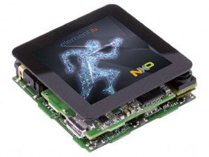
Fully-featured Android and Linux operating system builds are provided, easing development effort for software developers, while also supporting extensive UI capabilities, powerful application software and connectivity stacks. All the source code is provided of course, so you do have the option of modifying the build of the open-source operating system yourself, if you need to customise it.

The WaRP7 development platform could be a powerful new player in the busy development board space, especially in wireless connectivity and wearable IoT applications where more computing power and an operating system such as Linux is required. 

 
Its combination of tiny size, strong performance, focus on power efficiency and integration with a powerful suite of onboard peripherals – along with Linux or Android support, make it uniquely placed to offer value in a lot of different IoT and wearable application areas.

With the array of features, the WaRP7 could be the platform for your next Internet of Things product – and we’re ready to help turn your WaRP7 ideas into reality.

Here at the LX Group we have the systems in both hardware and software to make your IoT vision a success. We have end-to-end experience and demonstrated results in the entire process of IoT product development, and we’re ready to help bring your existing or new product ideas to life. Getting started is easy – click here to contact us, telephone 1800 810 124, or just keep in the loop by connecting here.

LX is an award-winning electronics design company based in Sydney, Australia. LX services include full turnkey design, electronics, hardware, software and firmware design. LX specialises in IoT embedded systems and wireless technologies design.

Published by LX Pty Ltd for itself and the LX Group of companies, including LX Design House, LX Solutions and LX Consulting, LX Innovations.

Muhammad AwaisWearable Internet of Things products made easy with NXP WaRP7

The new JN5169 series of wireless microcontrollers from NXP is a range of low-power, high-performance RF microcontroller devices aimed at home automation and remote control, smart energy management, smart lighting and similar Internet-of-Things applications, particularly in consumer products as well as industrial environments.

These system-on-chip devices incorporate an enhanced 32-bit RISC processor and a comprehensive set of analog and digital peripherals along with an IEEE 802.15.4-compliant 2.4 GHz radio transceiver supporting the JenNet-IP, RF4CE and ZigBee Pro wireless networking standards. The 802.15.4/ZigBee network stack includes support for the ZigBee Light Link, ZigBee Smart Energy and ZigBee Home Automation profiles.

The JN5169 platform is Thread and ZigBee 3.0 ready, and it features a new toolchain for software development that offers extensive debugging capabilities while also allowing a reduction of up to 15% in compiled code size.

This family of devices have the ability to connect with up to 250 other nodes in a wireless mesh network, allowing them to be used in a variety of different mesh network and Internet-of-Things applications, from home automation and consumer electronics through to large-scale industrial applications.

There’s three chips in the new family, with different memory configurations to suit a range of applications – such as up to 512 kB of embedded Flash memory, up to 32 kB of RAM and 4 kB of on-board EEPROM. With up to 512 kB of flash on board, there is enough memory available to enable wireless over-the-air firmware updates.

This makes it easy to keep devices up-to-date with new features and security updates without the cost of additional external flash and without the need to replace or remove hardware devices in the field as new software updates are released.

The JN5169 is equipped with hardware peripherals to support a wide range of applications, including an I2C interface, an SPI port which can operate as either master or slave, up to 8 ADC channels with a built-in battery voltage monitor, a temperature sensor and support for either a 100-switch keyboard matrix or a 20-key capacitive touch pad.

The device also incorporates up to 20 digital I/O pins, a 128-bit AES security processor and integrated support for an infrared remote control transmitter, allowing remote control of devices such as air conditioners that use an infrared remote control.

Power use is incredibly low – the JN5169 series offers a very low receive current of just 14 milliamps, or as low as 0.6 micro amps in sleep mode – helping to keep standby power consumption low in household products such as smart lighting and to enable extended operation from small batteries in portable, battery-powered applications.

Furthermore, with a programmable clock speed capability – the JN5169 series can minimise power consumption in power-sensitive, battery-powered applications. Despite these strong energy efficiency features, an on-chip +10dBm power amplifier provides the JN5169 series with a transmission range that is double that of NXP’s existing RF home automation solutions, while drawing just 20 milliamps of current in transmit mode.

This is 40% lower than similar products currently on the market, according to NXP. Antenna diversity is also supported, maximising wireless performance and range while minimising energy use. NXP is also offering a series of new reference designs for network-connected smart lighting solutions based around the JN5169, including white, tuneable white and RGBW colour-programmable Internet-of-Things lighting solutions.

jennic2

These smart lighting reference designs are complemented by a range of other reference designs from NXP such as wireless switches, wall panel controls, smart plugs, IoT sensors and gateways, along with cloud services for controlling them that will be offered by NXP’s partners, making up a complete Internet-of-Things ecosystem.

Along with the use of the highly integrated JN5819 system-on-chip, these reference designs incorporate innovations such as the use of oscillator crystals rated for 85 degrees C rather than more expensive crystals specified for operation up to 125 degrees C.

Innovative hardware and software techniques incorporated in the JN5819 family allow the clock to be stable in high-temperature environments where these cheaper crystals are used. Design innovations such as these mean that NXP’s JN5169-based smart lighting reference designs have a reduction in total hardware cost of up to 25% compared to similar products on the market.

The JN5169 series also offers innovative solutions to the problem of setting up and commissioning IoT products in a user-friendly and secure way. These devices support near-field communications for device commissioning, making it easy and intuitive to provision new devices and set them up on the network with just a tap on an NFC-enabled smartphone or other device.

Using NFC connectivity for device commissioning is convenient and it also offers security benefits, allowing devices to be easily yet securely paired without broadcasting network details over the air.

This new JN5169 chipset from NXP will offer a new dimension in wireless home automation, and here at the LX Group we’re ready to bring your products to life. Getting started is easy – click here to contact us, or telephone 1800 810 124.

LX is an award-winning electronics design company based in Sydney, Australia. LX services include full turnkey design, electronics, hardware, software and firmware design. LX specialises in embedded systems and wireless technologies design.

Published by LX Pty Ltd for itself and the LX Group of companies, including LX Design House, LX Solutions and LX Consulting, LX Innovations.

Muhammad AwaisLow-power wireless home automation with the new NXP JN5169

As mentioned in our previous discussion of the 4-20 mA current loop, there are many forms of wired data transmission that can be used in products, and today we’d like to review another form – the Inter-integrated Circuit bus (or I2C bus for short). This is also known as the “two wire interface” and has been around for quite some time. Invented by NXP (previously Philips Semiconductor) the I2C bus is a multi-master serial single-ended data bus used to allow systems to communicate with a huge variety of electronic devices.

From a hardware perspective it is quite simple – each device connects to the serial data and clock lines, which are controlled by the master device. The clock and data lines are connected to Vdd via pull-up resistors, for example:

 The master device controls the bus clock and initiates communications with each slave device. Communications are initiated by sending the slave device address – which is unique to each device – and then either data write or request commands. Then the slave device will act upon received data, or broadcase the required number of bytes of data back to the master device.

You may be wondering how the slave addresses are organised – each device manufacturer applies for an address range from NXP for their products. Some devices will only have one set address, and some can have their address altered – for example by changing the last three bits in the binary representation of the addresses. This is done in hardware by connecting three pins to Vdd or GND.

The speed of the I2C bus varies, and can range from 10 kbps to 3.4Mbps – with the speed usually proportional to the total device power requirements. The usual speed for the majority of devices is 100 kbps.

The decision to use the I2C bus can be simple, due to the popularity of the interface even on the most inexpensive of microcontrollers – and many design engineeers are familiar with the bus due to the history.

But what sort of devices can make use of the I2C bus? There are literally thousands available, in a wide range of categories. These can include simple temperature sensors, EEPROMS, motor controllers, LCD interfaces, I/O expanders, real-time clocks, UART interfaces, ADC/DACs, and more.

Apart from the huge range of devices, the advantages of using the I2C bus include industry expertise, the ability to address literally hundreds of devices using only two master I/O pins, and that devices on the bus can be “hot swap” – that is you can add or remove devices from the bus without powering off the entire system. This in itself is perfect for systems with maximum run-time requirements, as technicians can replace faulty device modules with reduced down-time for the end user.

However there are disadvantages to the I2C bus, two of which need to be taken into consideration. The first is that the maximum physical length of a bus run is usually around 20 metres, and in some cases much less. You can use bus extension devices from NXP (and others) that will allow much further physical distances – however designers need to ensure the capacitance across the bus stays at around 400 picofarads.

The second disadvantage is the possibility of slave address clash. You may have two specialised devices with the same slave address. In these situations you need to use an address multiplexer IC on the bus which first needs to be controlled, and then the device selected is addressed as normal. Nevertheless, as part of normal prototyping and planning these disadvantages can be removed or minimised with appropriate engineering.

It can be said that the I2C data bus may not be the “latest technology”, but it can effectively solve problems in the right circumstances. However there are many options, and choosing the right one is a fundamental step for the success of your project. So if your design team is set in their ways, or you’re not sure which data communication method is best for your application – it’s time to discuss this with independent, experienced engineers.

 At the LX Group we have experience designing a wide range of data gathering and control systems over short and long distances – and using this experience we can determine the most effective method of returning data and control signals no matter the application or geography. Our engineering team have developed a number of systems in this area and have extensive experience with the core technology requirements of such systems.

We understand the importance of high availability, accuracy and integrity of the systems, combined with the need for future proofing infrastructure rollouts. For more information or a confidential discussion about your ideas and how we can help bring them to life – click here to contact us, or telephone 1800 810 124.

LX is an award-winning electronics design company based in Sydney, Australia. LX services include full turnkey design, electronics, hardware, software and firmware design. LX specialises in embedded systems and wireless technologies design. https://lx-group.com.au  Published by LX Pty Ltd for itself and the LX Group of companies, including LX Design House, LX Solutions and LX Consulting, LX Innovations.
Muhammad AwaisLX Group discusses the Inter-integrated Circuit Bus